production workmanship
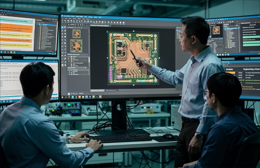
Design & DFM Check
This is the starting point of all work. After engineers use professional software such as Altium Designer to complete PCB design, they will generate manufacturing files in formats such as Gerber. After receiving the documents, the factory will conduct a strict manufacturability review to check whether the line width, line spacing, aperture, etc. meet the process capability, just like an architect reviews whether the drawings are feasible. This step can detect and solve problems in advance, avoiding subsequent losses.
Inner Layer Fabrication
After cleaning, the copper-clad board is coated with a photosensitive dry film. The designed circuit artwork is then aligned and exposed to ultraviolet light, causing the exposed areas of the film to harden and protect the underlying copper. The unhardened film is removed, and the exposed copper is chemically etched away, leaving only the required circuit pattern. Finally, the remaining protective film is stripped off, and the finished circuitry is inspected using Automatic Optical Inspection (AOI) to verify compliance with the original design and ensure defect-free production.
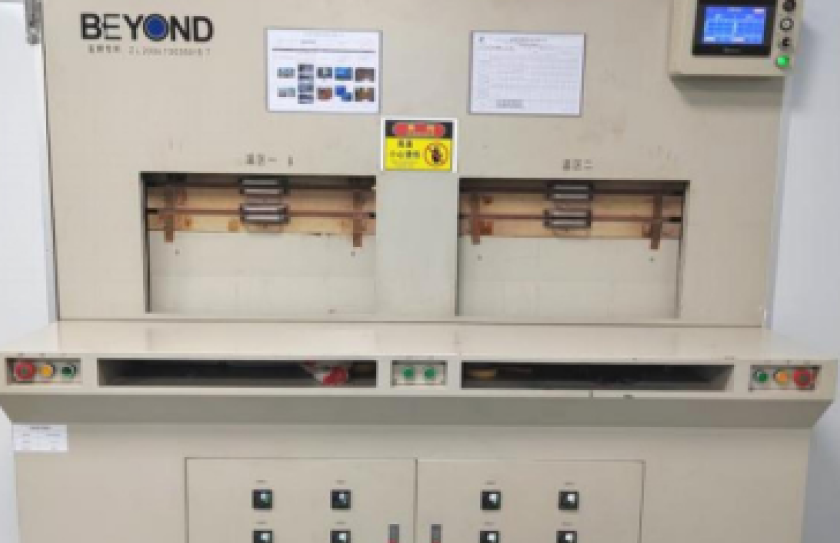
Lamination
This is a crucial step in manufacturing multilayer boards. Align and stack the produced inner core board, semi cured sheet, and outer copper foil accurately like a "sandwich biscuit", and then send them to a vacuum hot press machine. Under high temperature and pressure, the semi cured sheet melts and solidifies, firmly bonding all layers into a whole.
Drilling
Using a high-precision CNC drilling machine, drill through holes and component insertion holes on the board to connect different layers of circuits according to the design documents. For micro blind holes like those in HDI boards, more precise laser drilling machines will be used. The accuracy of drilling directly affects whether the circuit can be connected correctly.
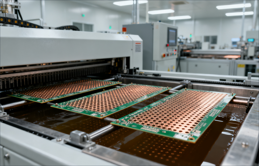
Plated Through Hole
The wall of the drilled hole is insulated and needs to be made conductive. This step involves a series of chemical treatments, depositing a thin layer of chemical copper on the hole wall, and then thickening the copper layer through electroplating to achieve electrical interconnection between different layers of circuits.
Outer Layer Pattern
& Plating
The production of outer circuit usually adopts positive film technology. Similar to the inner layer, a photosensitive film is also attached to the surface and exposed. But the difference is that the parts of the circuit that need to be preserved will be electroplated with copper and tin, with the tin layer serving as a protective layer. Then remove the photosensitive film, use etching solution to remove the copper foil in the non circuit area, and finally remove the tin to expose the final outer circuit.
Solder Mask & Silkscreen
Solder mask: commonly known as "green oil", is a protective coating. It covers the wire and only exposes the solder pads that need to be welded, which can prevent short circuits and oxidation during welding. The coating colors here include (blue, white, red, etc., different colors can be used according to customer product requirements).
Screen printing layer: On top of the solder mask layer, the identification, symbols, board numbers, and other information of the components are printed with white or other colored ink to facilitate subsequent assembly and maintenance.
Surface Finish
In order to protect the exposed copper surface of the solder pad from oxidation and ensure good welding performance, surface treatment is required for the solder pad. Common ways include:
Tin spraying: Low cost, good welding performance, but slightly poor surface smoothness.
Sinking gold: with a smooth surface and long storage time, commonly used for gold fingers and precision component boards.
OSP: Low cost, simple process, but short shelf life.
Routing, Testing
& Inspection
Molding: Use a CNC milling machine to cut the entire production panel into individual small plates.
Electrical testing: Conduct 100% on/off testing through flying needle testing or specialized testing racks to ensure there are no functional defects such as open circuits or short circuits.
Final inspection: Conduct a final inspection of the appearance, size, and other aspects of the finished board. Once it is qualified, it can be packaged and shipped.
Summary and Expansion
Overall, the production of PCBs is a highly demanding precision manufacturing process that is interdependent. With the development of electronic products towards higher performance and smaller size, PCB technology is also constantly advancing. Advanced processes such as arbitrary layer interconnects and embedded components have gradually been applied to high-end products.